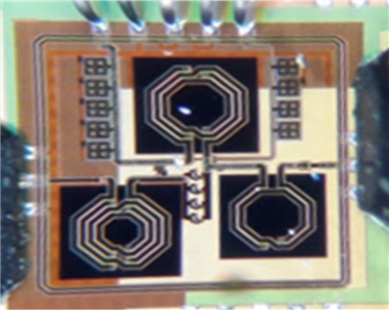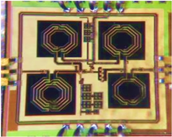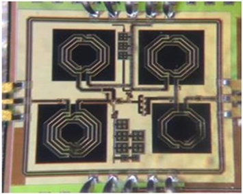

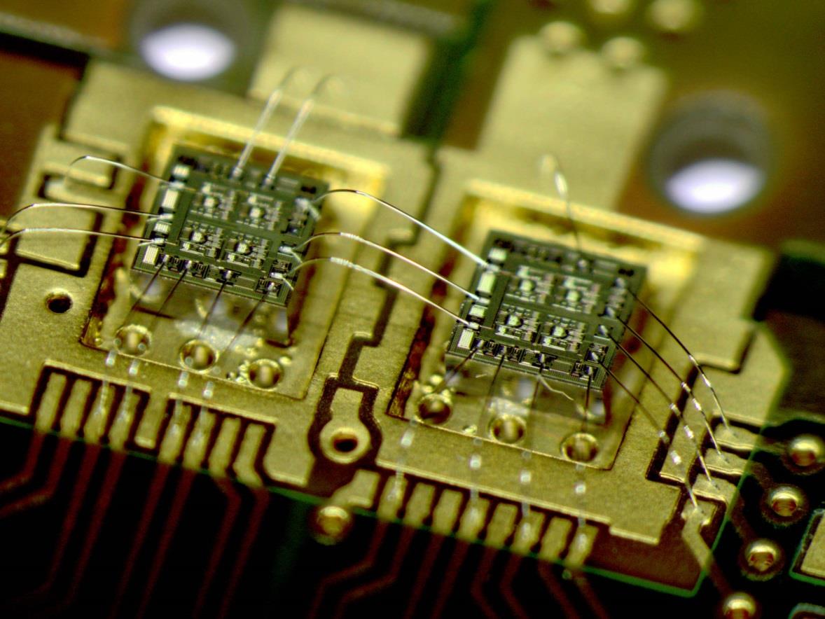

We provide IPs of various CMOS RF and Analog circuits such as power amplifiers, low noise amplifiers, voltage controlled oscillators, mixers, transceivers, transmitters and receivers that are designed in various CMOS technology nodes and operates for various specifications.
We also provide custom schematic and layout design services for RF and Analog Integrated Circuits. Complete design work flow from schematic level simulations up to post-layout simulations with complete data are provided to the customers.
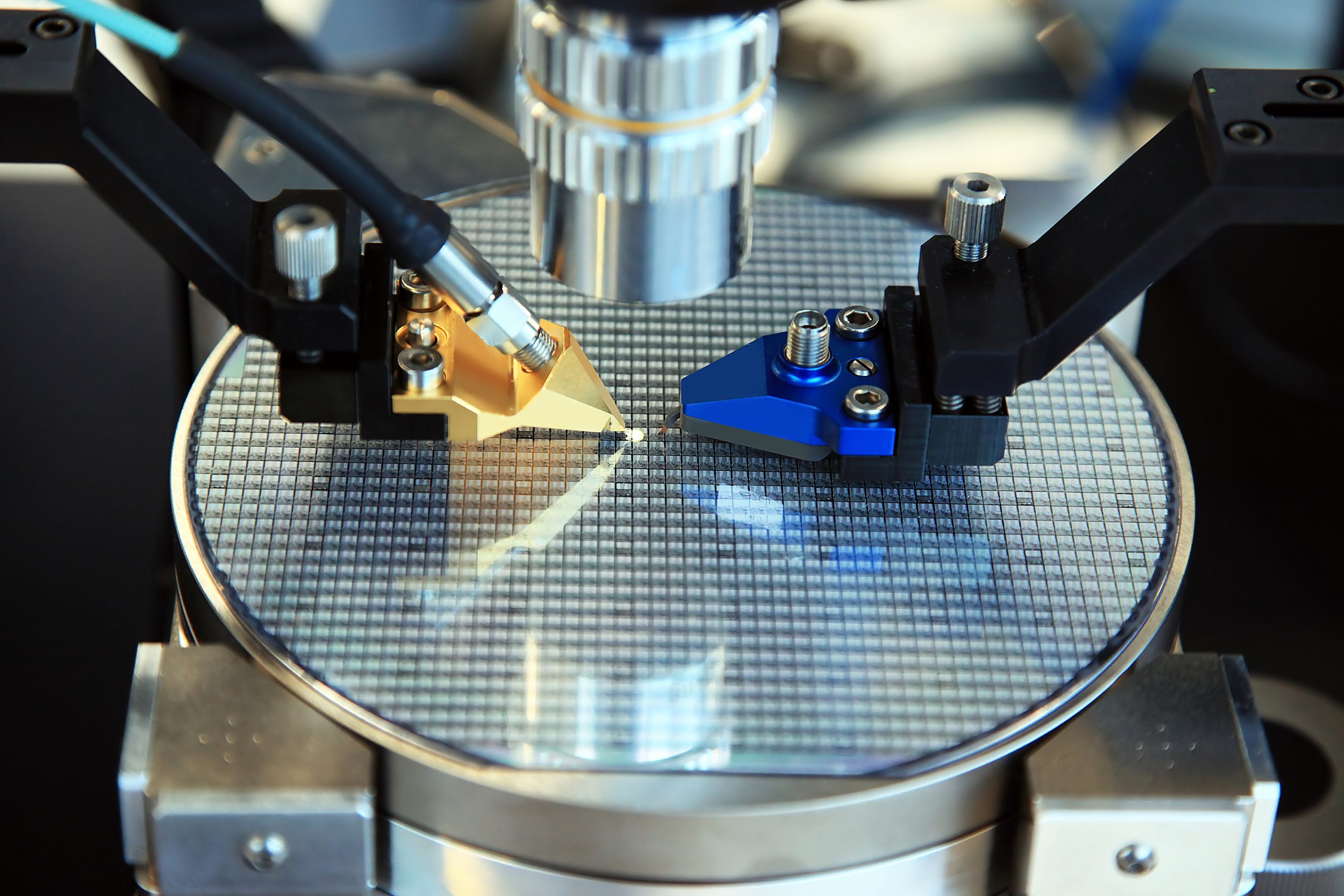
We also engage in technical and troubleshooting supports for customer’s designs in terms of Design Rule Check (DRC) clear up, Layout vs Schematic (LVS) checking, Electromagnetic (EM) simulations, and on-field supports including simulations and measurements.
PCB designs are one of the key services that we provide. PCB layout designing, EM simulations, and on board troubleshootings are provided by our lead technical experts.
Power amplifier, low noise amplifier, voltage controlled oscillator, and mixer circuits design trainings are conducted by our leading experts for students and engineers who are keen to learn IC designs. Participants will be trained and exposed on the complete flow of design simulations from schematic level up to layout extraction and a certificate of participation will be given upon completion of the training.
Having difficulty in getting your work published? We can assist you. With numerous publications in low and high impact factor journals and articles by our leading experts in RFIC designs, we can provide you consultancy on journals and articles writings which can assist you in publishing your work.
To provide the best solution in IC Design.
Document providing the specifications for our products.